Jump to content


routerbad's Content

There have been 1000 items by routerbad (Search limited from 08-June 23)


By content type

See this member's


Sort by                Order  

#167359 [Photo] Wii U GPU Die

Posted by routerbad on 05 February 2013 - 04:37 PM in Wii U Hardware

R700 is still ATI branded! So i dont think its R700 at all! Its custom, but SPUs can be older with 20 ALUs on SPU, so we get a nuber of 160 spus @ 550MHz is 176 gflops.

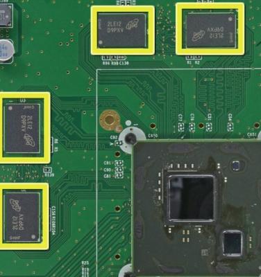
Right, if it was based on R700 it would carry ATi branding as well. Going on the assumption that this chip is completely custom then really anything is possible. The consensus at the moment is 40 ALUs/SPU for 320 SPUs @ 352GFLOPS.

e6760 has 480 sp's @600MHz. You think they just used the SPU's from that chip and customized everything else?


#171914 [Photo] Wii U GPU Die

Posted by routerbad on 15 February 2013 - 07:58 PM in Wii U Hardware

But so, how much the ps4 and new xbox will be better? the difference can be a wii vs 360/ps3? a psone vs n64? a dreamcast vs ps2, a dreamcast vs gamecube or xbox, or ps2 vs xbox.. i mean, where wii u can fit in a comparison like these? Is there any sure about the other specs?

They're better specwise, but not much. How that will translate into games, we won't know until we know.


#171768 [Photo] Wii U GPU Die

Posted by routerbad on 15 February 2013 - 09:50 AM in Wii U Hardware

a lot more cache/core, it no doubt has additional and more modern instructions. I can't help but wonder if they are using a stronger FPU or have updated the SIMD logic at all.


#181926 [Photo] Wii U GPU Die

Posted by routerbad on 12 March 2013 - 09:01 AM in Wii U Hardware

So can anyone calculate the specs if an E6760 was under-clocked by 50hz and used DDR3 RAM instead of GDDR5 RAM?

Well, E6760 doesn't come with 32MB of SRAM on the die, so the memory bandwidth and latency are just about as good as you can get.  DDR3 can pool resources just fine, and the SRAM is about the fastest RAM in existence and will be doing the majority of swaps with mem2.


Memory bandwidth aside, I've already laid out what we're looking at strictly from the programmable shaders power wise.  We can't know or calclate what the dedicated silicon is doing.  bgassassin on neogaf still thinks its performance will be equivalent to just over 1TFLOP when accounting for fixed functions, dedicated silicon, shaders, etc based on his industry source. 


#181967 [Photo] Wii U GPU Die

Posted by routerbad on 12 March 2013 - 11:55 AM in Wii U Hardware

A TFLOP at 550Mhz?! Madness....

Yeah that isn't the actual number, it was just mentioned that it performs that way, when the features of the GPU are put to good use.  You can only really calculate flops based on programmable shaders, unless you know exactly what's going on in the rest of the logic, and that would put us somewhere in the 500GFLOP range based on what we know about the E6760.  Because it has one less SIMD engine than a stock E6760 and that GPU comes in at 576GFLOPS stock 


Ok BUT can anyone accurately to close to accurately predict the Specs of the Wii U and compare it to what the PS360 can do, and compare it on what the PS4 can do.


It's obvious the PS4 will be able to do more, but how much more? I know the gap is apparently small, but how much smaller? I'm not trying to bash the GPU in the Wii U I'm actually trying to do the opposite, but without much effect heh


The GPGPU is able to do stuff the CPU used to do in current gen consoles. Does this mean the CPU in the Wii U uses it's cores for the gamepad and OS instead? 

we are in diminishing returns territory, meaning that more polygons =/= better looking graphics.  The gap is small already, and once you take into account that the increased performance isn't going to mean better graphics it becomes even smaller.  PS4 will still win out performance wise, and we'll likely see games toward the end of the gen that run smoother on that console than on Wii U, and maybe some that look marginally better, though not enough to change the experience.


#182059 [Photo] Wii U GPU Die

Posted by routerbad on 12 March 2013 - 03:12 PM in Wii U Hardware

Because it looks like it'd be too complex to explain how the Wii U running at a low clock can perform so well. It'd be easier to show people a visual example, or have a piece of demo software running on Unreal 4 or something like that. It's a simple and easier way to explain specs rather than raw numbers

Honestly I don't think they really know exactly what the specs are.


#182046 [Photo] Wii U GPU Die

Posted by routerbad on 12 March 2013 - 02:58 PM in Wii U Hardware

why don't Nintendo just come out with the specs.

I have no idea.  Then again, because their design strategy doesn't focus on raw power, it wouldn't be in their best interest to do that.


#170215 [Photo] Wii U GPU Die

Posted by routerbad on 11 February 2013 - 12:25 PM in Wii U Hardware

so devs dont even have info. supports working on the GPU/CPU desing all the way up to the last second. im beginning to wonder if nintendo is trying to make there games look bad, to set a low bar for early games next to other consuls, then all of a sudden BAM, we lied. there is some support but it is still a out-there theory.

no CPU die shots yet... how?


I wonder why no one else has thought of the obvious reasons they might have intentionally withheld serious specifications. To keep the competition in the dark! Durango leaked specs with 8GB of ram, then the rumor mill starts churning out claims that Sony is upping the RAM to stay competitive. No one can leak Nintendo info if very few people have it. I think the negative press it is getting is a result of not working with the videogaming media, they are peeved at Nintendo for keeping them in the dark because they feel entitled to every little detail.

Now that the competition's specs have been finalized (once they are confirmed to be so) I expect Nintendo to come out with all of the information they have on the hardware. If I were them, I would keep it away from VG media as much as possible, and let what the devs are able to do with the system provide all the evidence needed of it's potential.

The only other reason I can think of is they gave all the information they themselves had at the time, given the highly customized nature of the architecture and the lack of comparable chips or code to baseline performance on, I wouldn't doubt this either. It seems they only finalized the hardware within several months of the launch, and in that time their own dev groups had to figure out what they had to work with.

No CPU shots yet, they are forthcoming.


#173312 [Photo] Wii U GPU Die

Posted by routerbad on 19 February 2013 - 10:07 PM in Wii U Hardware

thats why I gave u the last link... they seperate them to AMD and ATI (5xxx and backwrds)


Interesting.  I've said multiple times here that i think that its the e6760.  It fits the process, the power profile, the performance profile, everything.  Because no one has a die shot of a e6760 we can't know for sure, but it's pretty clear none of the r700 series cards really fit the bill.


#167435 [Photo] Wii U GPU Die

Posted by routerbad on 05 February 2013 - 07:05 PM in Wii U Hardware

So you don't account for the number of SP's per SIMD core?


#167381 [Photo] Wii U GPU Die

Posted by routerbad on 05 February 2013 - 05:18 PM in Wii U Hardware

Looks like AMD changed all of the nomenclature. Each SIMD has 16 SP's, each SP has 5 processing elements, if they are using evergreen SIMD cores that would be 8 (that we know of) simd cores with a total of 640 processing elements.e6760 only has 6 SIMD cores and 480 PEs.

That would put it at 352 GFLOPS which doesn't make sense to me because the same calculation would cut the e6760 GFLOPS from 576 to ~288 (did it a minute ago, can't remember exact number)

Does SIMD width come into the calculation at all? What am I missing here?

I'll have to look at that a little later, have to head home from work.


#169189 [Photo] Wii U GPU Die

Posted by routerbad on 09 February 2013 - 09:31 AM in Wii U Hardware

What is Wii U's bandwidth now with this GPU info when not relying on eDram? Just wondering if the 12.8 GB from anandtech is correct or not.


12.8GB/s for the DDR3, Anandtech had no info on the 140GB/s EDRAM in the GPU. Wii U definitely has the most complicated, and the most tightly designed memory architecture out of all of the 8th gen consoles.


#167820 [Photo] Wii U GPU Die

Posted by routerbad on 06 February 2013 - 04:26 PM in Wii U Hardware

So BGAssassin still thinks we're looking at around 1TF or more taking "dedicated solicon" into account. He wouldn't label it fixed function, though that's what I would suppose that amounts to. Very interesting post.


#167366 [Photo] Wii U GPU Die

Posted by routerbad on 05 February 2013 - 04:54 PM in Wii U Hardware

So it isnt based on VLIW at all then? Do we know for sure AMD provided them or is that speculation? That would change the conversation drastically I think because everyone is assuming that the 8 clearly visible SPU's are based on VLIW5.


#168505 [Photo] Wii U GPU Die

Posted by routerbad on 07 February 2013 - 07:28 PM in Wii U Hardware

well i expect gc/xbox like gen 3 rd parties similar or better along with consul preformance. if ps4 flops as a inefficient steroids engine again then a even better match. think the GPU is ruffly even with RV770 main parts. but can be pushed alot more do to on die ram and custom parts to unload alot of work, hopefully leaving the main parts the basic build and custom on making it look nice. id design wii BC parts cabable of runnning with wiiu and not exclusivly wii. expect most games below par to 720/ps4 but some high end games at their upper limmit

I really think when it comes to actual visuals for games actually built for each of the next gen consoles, we'd be hard pressed to find any sizeable difference between the three. Sure Orbis and Durango are FLOPS monsters, but I doubt seriously either will be able to reach anywhere near peak, Orbis will have a harder time with it than Durango I think. I really think that all three systems give devs plenty of room to express themselves artistically, and all will have the ability to display some impressive stuff. Hell we've already seen some impressive stuff done on Wii U. Maybe it starts to show it's weaknesses at the end of the gen, but not most of it, and certainly not early on.


#168407 [Photo] Wii U GPU Die

Posted by routerbad on 07 February 2013 - 02:59 PM in Wii U Hardware

UE4 is made with nVidia GPUs in mind, almost all special effects are nVidia GPU exclusive ones, made possible by physix and cuda cores technology. All next gen consoles have AMD GPUs, so UE4 wont run in its full glory on any console!

P.S. I am AMD user, so no eye candy for me on my PC! :(


I'm an AMD user as well, so I guess I'm out as well. I need to get rid of my 6870's, slightly disappointed in them.


#167831 [Photo] Wii U GPU Die

Posted by routerbad on 06 February 2013 - 04:50 PM in Wii U Hardware

http://www.neogaf.co...&postcount=1663


*Comes out of his hole (again)*

I tend to forget some people take this stuff a lot more serious than I do.

First a thanks to Chipworks for going above and beyond for the picture and to blu, Durante, Fourth Storm, Thraktor, and wsippel for the work they did. Shinjohn let me know that the picture had been obtained and sent me a link, but I also checked out the thread. I wanted to come back and help with the confusion and what not.

As some of you know getting info about the hardware was a pain because what Nintendo released essentially boiled down to a features list. And by that I mean general features of a modern GPU that could easily be looked up. Info that dealt with performance apparently was not given out leaving devs to figure have to figure it out on their own. I had two working ideas of the GPU based on a more traditional design (which I was hoping for) and a non-traditional design. I see that some of you actually remembered the non-traditional idea. Wsippel and I would compare notes on whatever info we could come up with. Some of those notes led us to come up with how it may look if Nintendo took the non-traditional route.

http://www.neogaf.com/forum/showpost...ostcount=12053

In this post you’ll see both wsippel’s take and my take. I’m going to address some things in that post because I know some of you will try to take them out of context. First you’ll see wsippel’s baseline ended up being more accurate than mine. When I talked about the potential performance of 1TF or more that was in comparison to the R700 series because new GPUs are more efficient than that line, a higher baseline, and my idea focused on the dedicated silicon handling other performance tasks.

So what was the basis for the non-traditional view? I shared two of those bits of info before.

http://www.neogaf.com/forum/showpost...postcount=6136


Quote:
Well, I can't reveal too much. The performance target is still more or less the same as the last review from around E3. Now it's more balanced and "2012" now that it's nearer to complete and now AMD is providing proper stuff. As far as specs, I don't see any big change for better or worse, other than said cost/performance balance tweaks... It won't make a significant difference to the end user. As far as the kit goes, it's almost like what MS went through. Except more Japanese-ish... If you know what I mean.
http://www.neogaf.com/forum/showpost...postcount=6305


Quote:
Anyway, things are shaping up now with the new year. There was some anxiety with some less close third parties about what they were doing with GPU side, whether things were going to be left in the past... but it looks more modern now. You know, there simply wasn't actual U GPU data in third party hands this time last year, just the target range and R700 reference GPU for porting 360 titles to the new cafe control. Maybe now they finally can get to start debugging of the specifics and start showing a difference...
Here is one more specific piece that I didn’t fully share.


Quote:
I can't confirm or deny, sorry. The cat is very confidential and I repeat non-final. The target, last checked, is triple core with XX eDram and exclusive Nintendo instructions. 1080/30 capable Radeon HD w/tess. and exclusive Nintendo patented features. On a nice, tight bus that MS wishes they had on 360. ;)

I appreciate the individual for sharing as much as he did. He was a little paranoid though (I can understand) and at one point thought I was leaking info on a messageboard under a different name, but wouldn’t tell me the board or the username, lol.

I’m sure some of you remember me talking about games being 720p. It’s because with this I knew devs would use those resources for 720p development. I’m sure some of you also remember me mentioning the bus. The key thing in this is the “Nintendo patented features”. In the context of things we talked about, it seemed to me these were going to be hardwired features. What is certain for now is that the die shot shows a design that is not traditional, fewer ALUs (in number) from where things supposedly started with the first kit, and GPU logic that is unaccounted for. I’ve seen some saying fixed functions, but that’s too specific to be accurate right now. Dedicated silicon would be a better alternative to use, though I say that as a suggestion. In my opinion I think lighting is a part of this. The Zelda and Bird demos emphasized this. Also in the past it was discussed how Nintendo likes predictability of performance. It would also suggest Nintendo wasn’t ready to embrace a “fully” programmable GPU and kept on the water wings when jumping in the pool.

I did what I could to get as much info on the hardware as possible since Nintendo was giving out so little. From there I gave the best speculation I could based on that info. As of today, I still stand by the evaluations I made about Wii U’s potential performance from all the info I could gather. And until Nintendo’s games show otherwise I’ll continue to stand by them because in the end it’s on Nintendo show what Wii U is capable of.

And if you think I deserve flak for what I’ve said in the past then I’m here, but you’re wasting your time trying because my view hasn’t changed yet.

I made the farewell post to hold myself accountable to avoid posting, but I haven’t done well sticking to that, haha. I wasn’t going to make this post, but since I was one of the primary ones gathering info it’s unfair to you guys to leave things as they were.


#189812 Wii U's RAM is slower than PS3/Xbox 360.

Posted by routerbad on 03 April 2013 - 02:27 PM in Wii U Hardware


routerbad, on 03 Apr 2013 - 08:28, said:I think I may have gone overboard there, it wouldn't be an 88bit channel per chip, it would be 22 (44 per chip in dual channel mode) which would make the total bus 176.
If we go by that we have 800*2(data rate)*2(interfaces, or dual channel)*88 (bus width)/8 = 35,200Mb/s  I think that is the most reasonable number, and one you provided earlier.
Another way to look at it is 200*2*4*88/8 for 17.6 then double that for dual channel for the same number.


That makes my gut happy.

But these lanes... Somethins not right. Is their a memory controller inside those ram housings?

Yeah 12.8 wasn't sitting well with me either.


#191621 Wii U's RAM is slower than PS3/Xbox 360.

Posted by routerbad on 08 April 2013 - 01:26 PM in Wii U Hardware

Yea, the bandwidth to the edram on the Wii U would be higher.  The 360's edram wasnt really edram on the first versions of the 360, it was on a seperate chip that was placed onto the 360.  You sure about the 360 bandwidth, I read that it was cut in half for reads and writes.  Like I pointe out, a HD5450 can run Need For Speed Most Wanted and has only 12.8GB/s of bandwidth.  The bandwidth savings from edram is huge, so the Wii U would be in far better shape even with only 12.8GB/s to the main memory pool.  The edram is the performer here.  Its fast, and has enough capacity to hold the bandwidth hogs allowing the main memory to be used exclusively for reads.  Keep in mind that the 360 always has to send the framebuffer to the main memory before it can be sent out of display.  It also has to use tiling to do a 720p frame with AA, eating up even more bandwidth to the main memory.   

That's what we need numbers for, what is the bandwidth between Mem0 and Mem2, and how is the Wii U designed to use it?


I'm pretty sure about the 360 bandwidth, and the diagram shows that the 10GB/s number is for GPU/CPU communications.  if the edram was used correctly, as a go between between main ram and the GPU, if the bandwidth between the two RAM pools was high enough, theoretically the GPU would never need to directly read or write with main RAM.  if they can stream assets through the faster bus, as well as use some of that for the high bandwidth users, it would make the effective bandwidth much much higher.  Kind of like a lower cost way of creating GDDR like overall bandwidth (not really that high, but high enough to stay competitive) as well as keeping resource intensive functions off the GPU registers.  A best of both worlds.


#189806 Wii U's RAM is slower than PS3/Xbox 360.

Posted by routerbad on 03 April 2013 - 02:14 PM in Wii U Hardware


routerbad, on 03 Apr 2013 - 07:49, said:Aha, it would be 
Ahh, it would be 17.6 PER MODULE though, each module is on a separate 88 bit channel width.
Funny thing, 17.4 * 4 modules is 69.6, which isn't far off from what we've been saying.


----------------------------------
across 11 lanes per chip.... hmmmm.... I want to see the underside of the wii u motherboard.


routerbad, on 03 Apr 2013 - 07:49, said:Aha, it would be 
Ahh, it would be 17.6 PER MODULE though, each module is on a separate 88 bit channel width.
Funny thing, 17.6 * 4 modules is 70.4, which isn't far off from what we've been saying.
Basically the 800MHz number we are using for the memory clock rate rather than 200MHz is effectively giving us the same number based on four chips.  So I think goodtwins was correct with using 200MHz as the memory clock rate (though strangely the Micron website lists it as an 800MHz memory clock, not IO clock).  Going by that, we have:
200*2*4*88/8=17,600Mb/s * 4 Modules = 70,400Mb/s  exact same number 


Yeah, the memory clock was doing me in the head too. I wonder if one of the other ram suppliers is correctly listed.


----------------------------------------------
ah the underside of the wii u motherboard.

http://guide-images....VPDtCY6ppv.huge

I think I may have gone overboard there, it wouldn't be an 88bit channel per chip, it would be 22 (44 per chip in dual channel mode) which would make the total bus 176.


If we go by that we have 800*2(data rate)*2(interfaces, or dual channel)*88 (bus width)/8 = 35,200Mb/s  I think that is the most reasonable number, and one you provided earlier.


Another way to look at it is 200*2*4*88/8 for 17.6 then double that for dual channel for the same number.


#190122 Wii U's RAM is slower than PS3/Xbox 360.

Posted by routerbad on 04 April 2013 - 11:21 AM in Wii U Hardware

http://www.samsung.c...c-dram/overview


This is what throws a wrench into our theory though.  Notice that they are saying that with the x16 organization, the max bandwidth for the chip is 4.2GB/s, matching up to Anandtech's claim.  They arent saying per bank, but per chip.  It also matches up with PC's and the memory they use.  It would seem strange for graphics cards to have 8 memory chips on the card when four higher density chips could be used.  They are matching up the organization to the memory bus.  If the memory bus is 256 bit, you wont see anything less than 8 memory chips on board.  Eight chips times the x32 organization gives us the 256bit bus.  


Keep in mind that the Xbox 360 uses 8 seperate chips while the WIi U only has 4.  

Bit density in DDR3 should not effect bus width.


What we have are four modules, each is organized thusly, 256(rows)x16(columns)x8(banks).  This dictates how the memory is organized within the array itself, but the bus width per chip on a standard DDR3 interface is 32bit, or at least should be.


Didn't Hynix themselves confirm that each housing could support a 32 bit bus?


Goodtwin, on 04 Apr 2013 - 04:59, said:http://www.samsung.c...c-dram/overview
This is what throws a wrench into our theory though.  Notice that they are saying that with the x16 organization, the max bandwidth for the chip is 4.2GB/s, matching up to Anandtech's claim.  They arent saying per bank, but per chip.  It also matches up with PC's and the memory they use.  It would seem strange for graphics cards to have 8 memory chips on the card when four higher density chips could be used.  They are matching up the organization to the memory bus.  If the memory bus is 256 bit, you wont see anything less than 8 memory chips on board.  Eight chips times the x32 organization gives us the 256bit bus.  
Keep in mind that the Xbox 360 uses 8 seperate chips while the WIi U only has 4.  

xbox60_7.jpg

Were gravy dude.

Right, 360 only had four chips as well.  I still think that using the pin counts inside the GPU are going to be the best measure of the bus width.


Actually we have the answer to that.

256.

Found it when i found out the 360 uses the same ram chip as the wii u's samsung ram.

Samsung k4j52324qc-bc14

macroware.wordpress.com/2006/01/24/whats-inside-the-microsoft-xbox-360/

though the 360 only uses half the pins.

We dont know the pins on the ram side, but we know the pins where they plug in. 158 pins on the ddr3 io

1.6 * 158=252.8/8=31.6

31.6 GB/s

Its looking pretty rock solid.

Yeah, that lines up way too perfectly.  1.6 per pin, 158 pins.  We're golden.


#189344 Wii U's RAM is slower than PS3/Xbox 360.

Posted by routerbad on 02 April 2013 - 04:03 PM in Wii U Hardware


routerbad, on 02 Apr 2013 - 09:34, said:Yeah that notion is pretty much dead and gone.  
That should be DDR3 IO from the memory controller if I'm not mistaken, unless the memory controller is on the GPU with CPU interconnects.


It could be. i have no idea though, as all i can see is the lanes head into that corner, the mcm heat spreader hides everything from view, and the next step we have is the gpu itself. We still havent seen that middle ground.

It does look to be headed straight into the GPU from the angle on the mobo.  


gqSDvioKMCE2DKCr.huge_.jpg


Yep, straight into the GPU, unless the memory controller and entire northbridge is sitting on the MCM just outside the GPU.


#189295 Wii U's RAM is slower than PS3/Xbox 360.

Posted by routerbad on 02 April 2013 - 02:03 PM in Wii U Hardware

Just looked again at the Wii U motherboard.  The way the RAM bus lanes go into the MCM is consistent with memory controller IO (or even the entire northbridge IO) being concentrated on that corner of the MCM.  I don't see any reason why it wouldn't all be on the same bus, with software addressing restrictions in place to reserve RAM for system services.  I wonder if they could be trying to pull another N64 low/high res thing with us, albeit with a firmware update this time.


Goodtwin, on 02 Apr 2013 - 06:47, said:Ok, so 32bit is the maximum bus for ram modules.  I was assuming that it would be higher since there are high bandwidth memories like GDDR5, but apprently they get the bandwidth by having lots and lots of ram modules on the memory bus, and they run at way higher speeds than DDR3.  So if a graphics card for example has a 256bit memory bus, it would have to have eight 32bit ram modules to get maximum bandwidth.  If they were to use 16bit ram modules on that same graphics card, then there would have to be 16 ram modules on that memory bus.  I had to go look at some PC GPU's to see how in the world they were getting all that bandwidth.  Even when looking at GDDR5 memory on Hynix website, your going to notice that the bandwidth per brick of ram isnt that impressive, which was strange to me at first, but then I realized that bandwidth is simply a result of having lots of ram chips.  So having more low density ram modules instead of fewer high density ram modules is actually beneficial for bandwidth. 

Yes. Thats what the channesl mean. a 64 bit bus has 2 channels in that case. For 'natural' 64 bit busses, its just as simple, more lanes connect to the different modules inside the chip. Its called a double wide, but its just 2 32 bit busses. After all, all ram chips are made of smaller modules under 1 housing. wii u has a 128 bit bus, in this case. with half sent to games and half to system.

Interleaving helps reduce some of the clutter, but its not always practical, the 360 didnt use it because it was just too hot already, so the ram only had half the bandwidth for the number of modules it had.

there are 4 modules for each ram chip pair on the wii u.

with 2 channels we have a 64 bit bus, technically a 128 bit bus, but half is cut off.

anand tech said all 4 added up to 1 64 bit bus.

If you are saying hynix says 32bit per brick (standard for ddr3 2 channel, 64 bit), we are looking at a doubling of the bandwidth from anandtech.

Notice how the pairs of ram are connected by bus lanes to the back ends?

actually, reminds me of the ps4 ram. That also had 'paired' pools.

samsung%20ram%20(350%20x%20263).jpg

Huh. only 8 lines per chip. Wii u has 3 more lanes per chip on its bus.


eh, for some reason the wii u pic disappeared.


it has 11 lanes to its bus per chip vs ps3's 8.

even with the lane split we see on the PS3 in that image, they were able to unlock more RAM for developers, by lowering the OS footprint.


#189301 Wii U's RAM is slower than PS3/Xbox 360.

Posted by routerbad on 02 April 2013 - 02:07 PM in Wii U Hardware


routerbad, on 02 Apr 2013 - 08:17, said:Just looked again at the Wii U motherboard.  The way the RAM bus lanes go into the MCM is consistent with memory controller IO (or even the entire northbridge IO) being concentrated on that corner of the MCM.  I don't see any reason why it wouldn't all be on the same bus, with software addressing restrictions in place to reserve RAM for system services.  I wonder if they could be trying to pull another N64 low/high res thing with us, albeit with a firmware update this time.

even with the lane split we see on the PS3 in that image, they were able to unlock more RAM for developers, by lowering the OS footprint.


I dont think this 12.8 GB coffin can fit any more nails in it.

No, I think not.  Something is seriously wrong with the Anand teardown, whether it was bias, not enough coffee that morning, or just someone who didn't understand what they were looking at.  It isn't that far of a stretch though, 10 years of tracing leads on motherboards and there is still a lot of mystery in their design for me.


When I first started building electronics every setting was a manual jumper setting, so you had to become familiar with where jumper leads were going and what they did.


#189682 Wii U's RAM is slower than PS3/Xbox 360.

Posted by routerbad on 03 April 2013 - 11:45 AM in Wii U Hardware


Alex Atkin UK, on 03 Apr 2013 - 05:36, said:So what are we saying now then, potentially slightly under 4x the bandwidth of Xbox 360 (due to being clocked lower) as the Wii U might use 4 channels and likely at LEAST dual-channel?
I certainly have to agree that it would make little sense to have LESS bandwidth, and with the low-power architecture of the Wii U design overall I would be amazed if it wasn't at least dual-channel as its an almost free doubling of RAM bandwidth without drastically increasing the power/heat.


It DOES use 4 channels. We have pictures now, clear enough to know everything.

4 Chips of ram, 512 MB in each chip, each chip with its own bus, or 'channel'.

Each channel has 11 lanes, ddr3 gets 2 bits per clock from each lane.

Each channel is 22 bits. 4 channels makes for an 88 bit bus.

So you're basically getting 88bits per clock, per chip.  They are all going into the same memory controller, on the GPU.  we have a 352bit bus overall, and that entire bus is available for accessing RAM in game.  With one memory controller, and only software addressing restrictions, the memory controller can address the RAM in the most efficient way possible, which is alternating chips per address, to reduce refresh latency.  The Memory controller addresses it in this fashion, and creates an abstract address pool for software to access.  The games don't know how many memory controllers there are, all it recognizes are sequential memory addresses delivered from the controller.


Would that make it 17.6GB/s then?  800Mhz x 2 x 88= 17.6GB/s?  When you say channel, is that every line that you can see going from the ram modules to the MCM?

No, DDR3 is quad pumped, meaning you multiply the clock by 4 in the throughput calculation.


800 x 2 (bit channel) x 4 (clock multiplier) x 88 (bus width) / 8 (bits per byte)


I was using 700MHz in my calculations, but with 800 it comes to 70.4Gb/s


Dual Channel referring to the duplexing of the bus.


and he is referring to each chip being on it's own 11 lane channel. with 2 bits per lane.


Anti-Spam Bots!