I remember something along those lines from the nes article
Thanks for that!
Not worth the geeky soap? (discussion with Wii U developers)
Even if this “bandwidth drama” is only debated within confined circles, it shouldn’t be discarded, especially to gauge the Wii U longevity in regard to technically demanding third-party titles. To better comprehend this situation, we had a little chat with a developer (wishing to remain anonymous), who has released a graphically solid retail game on Wii U.
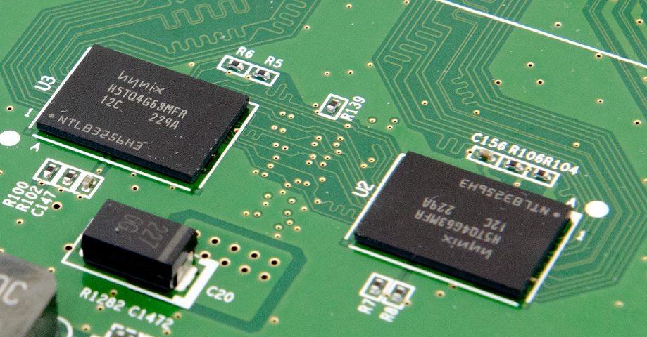
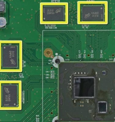
InquiringMind: The first teardowns of the system happened, and it seems the 2GB of ram are DDR3-1600 chips on a 64 bit bus, up to 43% slower than the RAM bandwidth of Xbox360 & PS3.
Anonymous developer: These numbers are not the actual Wii U memory performance. I wonder if such low specs would even make a port from XBox360 possible.
Do you mean there is more to it, that the dismantling may have overlooked something and in fact the bandwidth is higher? Or perhaps those rates are indeed true, but your observations on the overall memory performance are better, thanks to the eDram and caches?
I’m not capable of calculating memory throughput of DRAM chips like those websites nor I know the memory controller or how many channels such a controller uses or the actual timings of those chips. But when using the Wii U CPU caches properly to write memory from A to B then these numbers above get exceeded by far. And I don’t mean theoretical throughput on paper but real throughput in a game situation.
But are you strictly talking of the 1GB of RAM or the whole memory chain, including the CPU caches that you’re referring to here or even the eDram? And if it’s the first case, could you not be aware of some kind of mechanism involving the caches and the eDram that would automatically speed up the data from or into the RAM, and that would explains your higher measured numbers?
I talked about the 1GB. But if our results differ from the theoretical limits i think we simply measure different things.
So if I understand right, you have a way to know the speed of the RAM at your end, and what you’ve seen is clearly greater than 12GB/S? Would you say it’s in the same ballpark than the 22GB/s bandwidth of the Xbox360?
In my experience the Wii U surpasses any of these numbers under the right conditions. But as said, i can’t calculate the theoretical bandwidth of such DRAM, I can only talk about the actual system memory performance which is very good for me.
So according to Anandtech, more of the same DRAM array on a faster bus with more lanes equals half the throughput, because Nintendo.
Edited by routerbad, 03 April 2013 - 09:51 AM.


.jpg)